

Advanced Optical Sorting Systems in Electronic Component Manufacturing
2025-07-01 22:43Advanced Optical Sorting Systems in Electronic Component Manufacturing
Precision-Driven Quality Control for MLCCs, LTCCs, ICs, and Ferrite Cores

I. Industry Challenges & Technological Imperatives
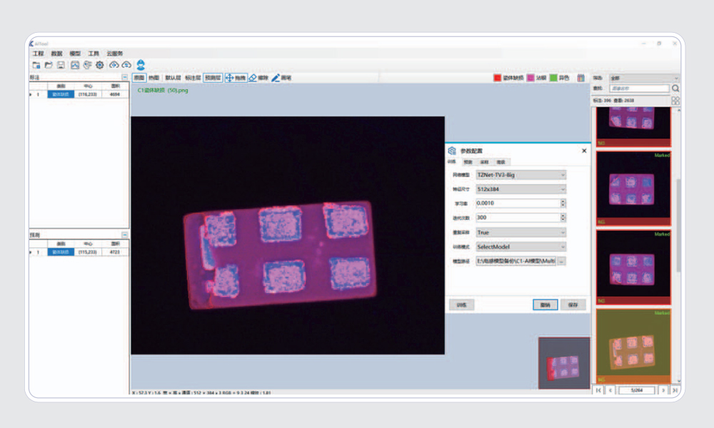
Electronic component manufacturing demands micron-level precision across high-volume production. As depicted in the provided image, miniature multilayered ceramic capacitors (MLCCs), low-temperature co-fired ceramics (LTCCs), chip-scale resistors/inductors, ICs, and ferrite cores require defect detection capabilities beyond human vision limits:
Tolerance Thresholds: MLCC electrode misalignment <5μm
Critical Defects: LTCC micro-cracks ≤20μm
Throughput Needs: SMD component sorting at >30,000 UPH
Optical sorting machines address these challenges by integrating hyperspectral imaging, deep learning, and robotic automation to replace error-prone manual inspection.
II. Component-Specific Optical Sorting Architectures
1. MLCC/LTCC Ceramic Components
Defect Detection:
∙ Surface pits/scratches → 5MP coaxial darkfield imaging
∙ Delamination → Terahertz wave subsurface tomography
∙ Electrode bleed → Color variance analysis (ΔE<0.1)Dimensional Verification:
∙ Laser triangulation for thickness (±2μm accuracy)
∙ Edge chipping detection via polygon-matching algorithms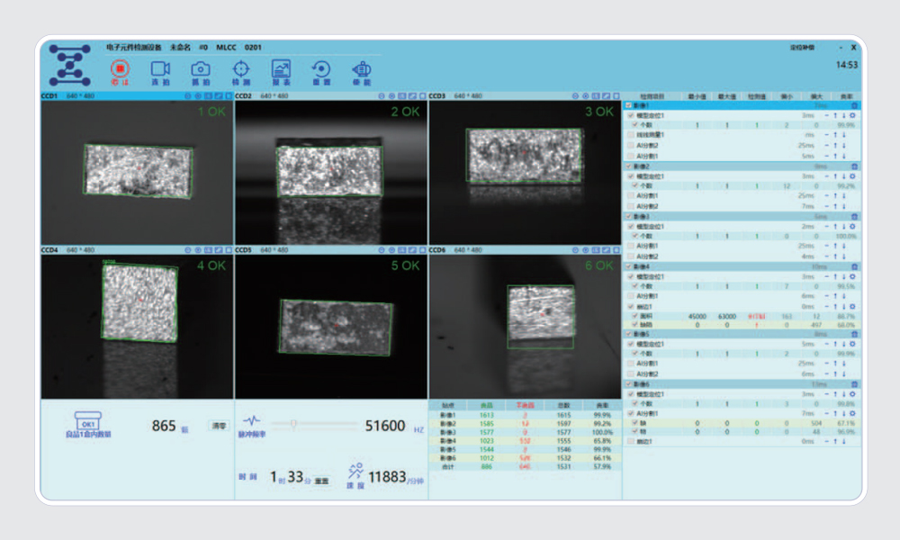
2. Chip Resistors/Inductors
Parameter Validation:
∙ Termination plating integrity → 20X optical microscopy
∙ Marking legibility → OCR with 99.97% read rate
∙ Coplanarity → 3D structured light (10nm Z-resolution)Performance Grading:
∙ TCR measurement via thermal imaging during stress testing
3. Integrated Circuits
Lead Frame Inspection:
∙ Pin coplanarity → Moiré interferometry
∙ Solder ball bridging → IR reflection analysis
∙ Wire bonding defects → 1μm-resolution X-ray laminographyContamination Control:
∙ Particulate detection down to ISO Class 3 standards
4. Ferrite Cores
(Image Reference: Bottom-left "Ferrite Core" section)
Material Integrity:
∙ Air gaps/cracks → Terahertz time-domain spectroscopy
∙ Dimensional accuracy → Shadow-free backlight metrology
∙ Coating uniformity → UV fluorescence imaging
III. Core Sorting System Technologies
A. Optical Subsystems
| Technology | Specifications | Component Applications |
|---|---|---|
| Hyperspectral Imaging | 400-1000nm range, 5nm resolution | Counterfeit material detection |
| Structured Light 3D | 5μm XY, 200nm Z accuracy | Solder paste height mapping |
| High-Speed TDI Camera | 32k lines/sec scan rate | Moving web inspection |
| Automated X-Y Theta | ±0.5μm positioning precision | Die attach verification |
B. AI-Driven Defect Recognition
Convolutional Neural Networks: Trained on >1M defect images
∙ Adaptive learning for new failure modes (e.g., tin whiskers)Anomaly Detection Algorithms:
∙ Unsupervised clustering for zero-defect validationParametric Correlation Engine:
∙ Relate optical defects to electrical performance (e.g., Q-factor degradation)
IV. Integration with Smart Manufacturing
1. Industry 4.0 Implementation
Equipment Interfacing:
∙ SECS/GEM protocols for real-time process adjustment
∙ FDC (Fault Detection Classification) integrationDigital Twin Simulation:
∙ Virtual sorting parameter optimization before physical runs
2. Automated Material Handling
Component-Specific Carriers:
∙ Vacuum end effectors for <1G acceleration shock
∙ Anti-static waffle trays with RFID tracking
V. Quantifiable Quality & Cost Benefits
| Metric | Before Optical Sorting | After Implementation |
|---|---|---|
| Defect Escape Rate | 820 PPM | 2.7 PPM |
| Inspection Speed | 5,000 UPH (manual) | 45,000 UPH |
| False Rejection | 18% | 0.3% |
| Rework Labor Cost | $18.50/kg | $1.20/kg |
Data Source: SEMI E178 global component manufacturing study
VI. Industry-Specific Case Studies
A. Automotive MLCC Production
Challenge: AEC-Q200 compliance requires 0 PPM cracks
Solution:
∙ Terahertz inline inspection with 99.999% coverage
∙ Multi-layer registration error detection <2μmOutcome:
∙ Achieved 0 field failures in 10M+ components
B. Medical IoT Chip Sorting
Challenge: Implantable device contamination control
Solution:
∙ ISO 14644-1 Class 4 cleanroom integration
∙ 0.1μm particulate monitoringOutcome:
∙ Passed FDA 21 CFR Part 11 audits with zero observations
VII. Standards Compliance
Electrical Testing: IEC 60384-1 (MLCCs), IEC 60195 (Ferrites)
Optical Calibration: ISO 5725 accuracy verification
Traceability: ASTM E2919 component-level data logging
VIII. Future Developments
Quantum Imaging Sensors: For sub-surface defect resolution beyond diffraction limits
Edge Computing Integration: Localized AI inference <5ms latency
Green Manufacturing: Sorting-guided material recovery (>95% precious metal reclamation)
Conclusion
Optical sorting machines have transformed electronic component manufacturing into a data-driven science. By deploying component-specific optical architectures as depicted in the image—from MLCC delamination detection to ferrite core structural analysis—manufacturers achieve unprecedented levels of quality assurance while reducing costs. The convergence of multi-modal imaging, Industry 4.0 connectivity, and adaptive AI ensures that optical sorters will remain pivotal in enabling next-generation electronics scaling, particularly for 5G, automotive electrification, and industrial IoT applications.